
신고사유
신고해주신 내용은 쇼핑몰 운영자의 검토 후 내부 운영 정책에 의해 처리가 진행됩니다.
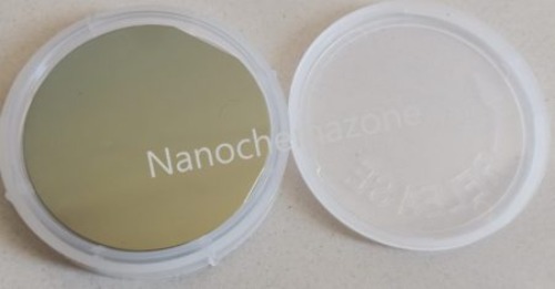
Single crystal silicon is the most widely used semiconductor material as a substrate material due to its excellent machinability, mechanical stability, and the potential to combine sensing elements and electronics on the same substrate. Circular wafers made of silicon are used as the substrate in most MEMS sensors. The crystal orientation should be known before manufacturing since silicon has orientation-dependent properties such as piezoresistivity coefficients and etching rates. The common orientation is (100) where the numbers represent Miller indices. As an example, (100) wafer that has a primary flat side as an indication of < 110 > direction. When a piezoresistive element is placed on a (100) wafer, the orientation should be parallel to < 110 > direction if the piezoresistivity coefficients in that direction are intended to be utilized.
Note: For pricing & ordering information, please contact us at sales@nanochemazone.com
Please contact us for quotes on Larger Quantities & Customization. E-mail: contact@nanochemazone.com
Customization: If you are planning to order large quantities for your industrial and academic needs, please note that customization of parameters (such as size, length, purity, functionalities, etc.) are available upon request.
Storage Conditions:
Airtight sealed, avoid light, and keep dry at room temperature.
게시물이 없습니다
게시물이 없습니다